- ARAB NEWS
- 15 Jul 2025

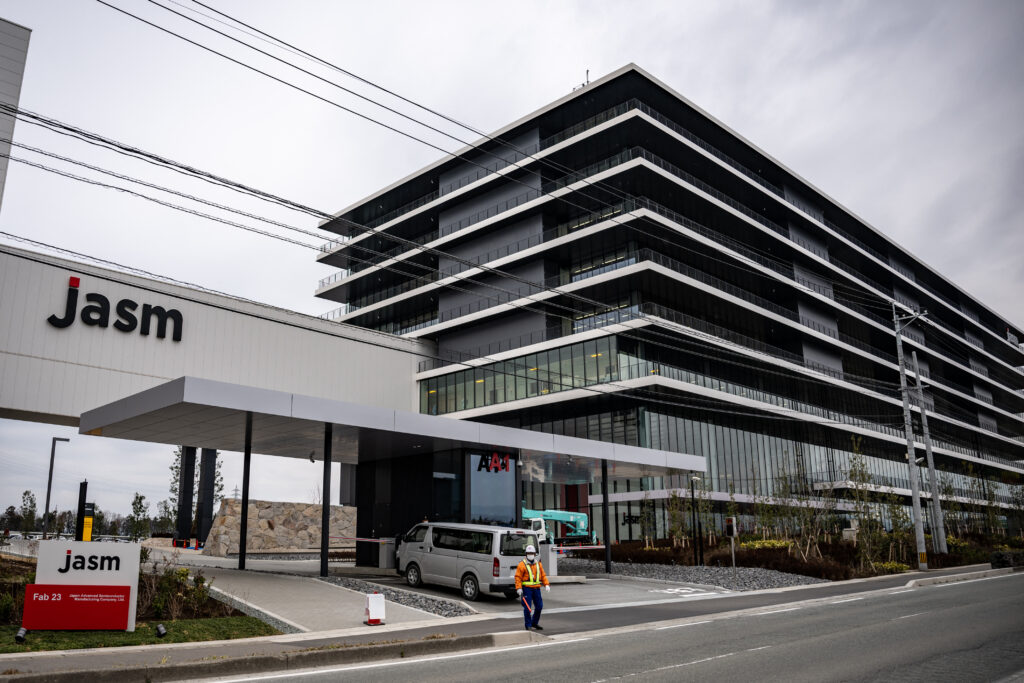
Kikuyo: Taiwan Semiconductor Manufacturing Co., the world’s largest contract chip foundry, on Saturday held an opening ceremony for its first plant in Japan, which was completed late last year and is set to be operational by the end of this year.
On the same day, Japan’s industry ministry said that it will provide up to 732 billion yen in financial aid for the Taiwanese company’s planned second plant in Japan.
The first plant is located in the town of Kikuyo, Kumamoto Prefecture. The second plant will also be built in the southwestern Japan prefecture.
The Japanese government’s financial aid for the two TSMC plants totals about 1.2 trillion yen, including up to 476 billion yen for the first plant, which it decided in 2022.
The aid comes as the government aims to support domestic production of semiconductors, which it views as an important item for economic security.
At the opening ceremony, TSMC founder Morris Chang said that the first plant will usher in the renaissance of semiconductor manufacturing in Japan.
In a video message, Japanese Prime Minister KISHIDA Fumio said the opening of the TSMC plant is “a great step forward for both our country’s semiconductor industry and user industries.”
Speaking to reporters after the ceremony, Japanese industry minister SAITO Ken mentioned the arrival of a “great era of global competition for semiconductor manufacturing capacity,” underscoring the need for massive government support.
The first plant, which has an area of roughly 21.3 hectares, will produce chips with circuit line widths of 12 to 28 nanometers, for use in smartphones and automobiles.
The opening ceremony was also attended by TSMC Chairman Mark Liu and Kumamoto Governor Ikuo Kabashima.
Prior to the ceremony, Saito met separately with Liu and Kabashima to discuss future support for the semiconductor industry.
Construction of the second plant is expected to begin later this year, and the plant is expected to be operational by the end of 2027.
Total investment in the two TSMC plants is expected to exceed 20 billion dollars, and the TSMC unit that will operate the plants will receive investments from Sony Semiconductor Solutions Corp., Denso Corp. and Toyota Motor Corp.
JIJI Press